Open
Description
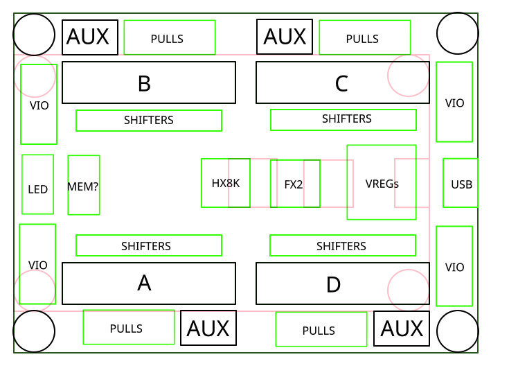
Summarizing the broad design points regarding revD in one place:
- Four I/O banks (ABCD) instead of two (AB)
- Placement of AB and CD so that addons developed for revC work on revD side by side (at least if width allows). That means relative position of AB and CD is the same as AB on revA-C.
- No LVDS bank.
- Goal: we should provide I2C and power to ports. Proposal#1: put I2C on NC pins in the 20-pin connector, put GND/3V3/GND/5V on a pin header next to 20-pin connector. Proposal#2: put SDA/SCL/GND/3V3/GND/5V on a pin header next to 20-pin connector, leave NC pins as NC.
- Goal: I2C on ports should not impact reliability due to faults such as stuck bus. Proposal: use 1:4 I2C level translating passthrough switch such as PCA9545A with dedicated reset pin.
- Problem: we run out of I2C addresses (definitely on PCA6408, possibly on DAC081 without change of package).
Proposal#1: change PCA6408 part and DAC081 package. Proposal#2: expand passthrough switch from (5) to 1:8, use identical parts to revC (simplifies production!).Proposal#3: Change only DAC081 package to allow four addresses. - Placement/layout sketch: https://marcan.st/transf/Screenshot_20190510_145158.png
- Proposal: replace ADC with INA233 to allow for precise current and voltage limiting (Replace ADC with INA233 #165). Existing 0.68 ohm resistor BOM line could be used for the shunt. Vsense range is also expanded to 0-36 V.
- Proposal addendum to (8): Connect INA233 ALERT pin directly to LDO EN pin, adding a resistor between FX2 GPIO and LDO EN. This way, any voltage or current fault condition will lead to immediate port shutdown, significantly improving safety.
- Consideration: if there is free board space, some sort of low pin count RAM would help with streaming workloads. Only a "nice to have" and should be dropped if troublesome at all. The RAM chip should be PSRAM, either QSPI or HyperRAM.
- Consideration: if there is still free board space left after (10), perhaps on underside, add a DNP footprint for SPI Flash connected in parallel to RAM.
- Proposal: expose Vref DAC output on extension connector from (4) to accomodate @electroniceel's advanced IO protection board.