Support for 256 page frames using an extra page register #5
Description
I've had an idea, looking at the source code of the driver and the original 2MB board schematics:
I've been looking at the Lo-tech EMS driver (in the software directory) for a bit.
I found out something: when it 'disables' a page frame (frame being IObase+0 through IObase+3), it simply writes 0xFF to the port.
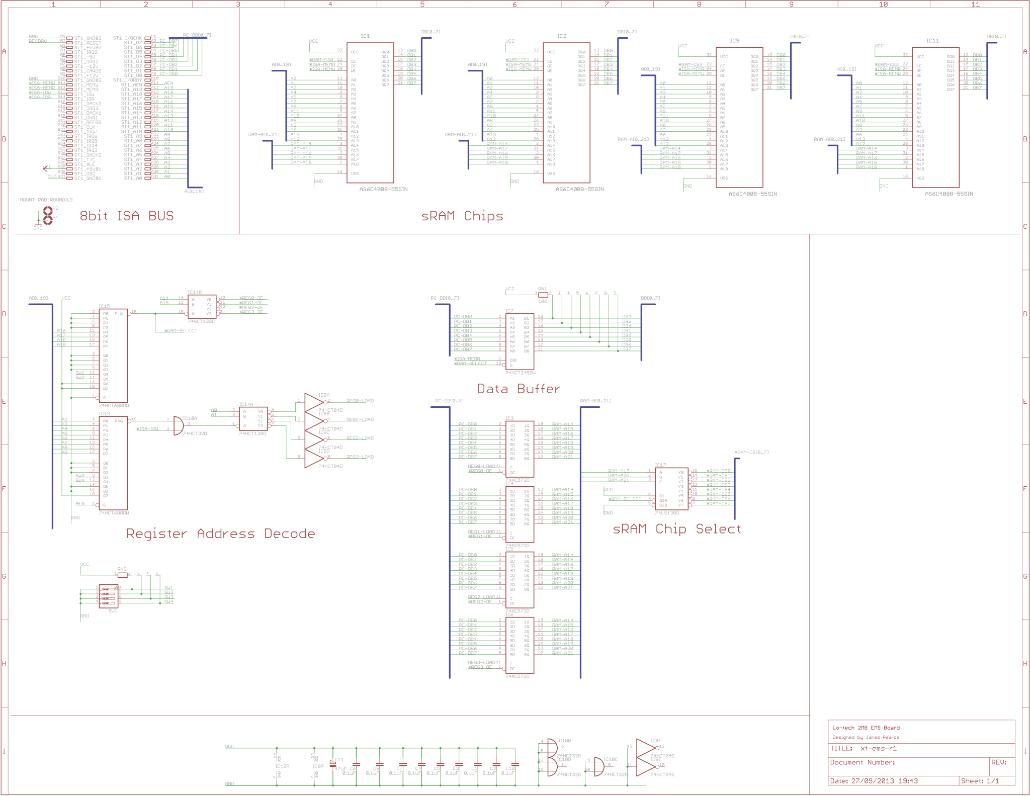
Then, looking at the board diagram (https://www.lo-tech.co.uk/w/images/7/73/Lo-tech-2MB-EMS-Board-schematic.png ) I see something interesting:
- The register outputs support full 256 page register values to be decoded onto 8 memory chips, thus 4MB. But, it only connects the first 4, thus setting bit 7 in the registers effectively 'disable' the memory (mapping to chips 4-7, which aren't connected), ignoring reads (floats the bus, thus 'unmapped') and writes don't respond?
Maybe someone could patch the board with an extra storage chip to set *RAM-SELECT (active low) based on *REG0-3OE (which are the inverted frame number bit in the added register to check, basically routed to address the added new register bit from a translation chip simply wire them to the output pins on another 74AC7530 chip like the page registers?), then use it's output bits to make (using a LUT ROM chip, address being the inputs):
Bit looked up(based on REG0-3OE (what window bit to inspect) and the added 74AC7530 chip for the 4MB enabled bit to use) - RAM-A21 - *RAM-SELECT INPUT -> *RAM-SELECT OUTPUT
Default result is 1(unmapped, all other of the 8 cases)
0 - 0 - 0 -> 0 (compatibility, <128 frame indexed)
1 - 1 - 0 -> 0 (4MB page addressed and enabled)
1 - 0 - 0 -> 0 (2MB page addressed and enabled in extended mode)
The only one cases remaining is not adressed and compatibility mode past 128(which is 'unmap page frame').
RAM-SELECT inputted from the 74HCT6880W and outputted to the sRAM CHIP SELECT chip.
So basically, put the new register at base address+4 for example. Then (programming it):
For unmapping: clear bit in register and set bit 7 in the page register (in compatibility mode now, so 2MB EMS compatible, bit 7 unmaps there due to chips 4-7 not being present, so emulate that here. Added bonus: like the original board, memory is unmapped with bit 7 set (since no RAM chips respond)).
For mapping enabled frame: clear bit in register and set page number below 127(compatibility with Lo-tech EMS driver), or set the window's bit (bit 0-3 for frame 0-3)) in register and set a 4MB page frame in the corresponding page register.
Although this is just theoretical. Any thoughts?
Edit: Or maybe more simple translation logic: include the 74AC7530 4-bit outputs in the LUT as well (requiring a 11-bit address for the ROM). So the translation ROM's address pins are connected to:
- RAM-A21 (high bit used)
- *RAM-SELECT input (memory address enable)
- REG0OE (reg0 memory addressed)
- REG10E (reg1 memory addressed)
- REG2OE (reg2 memory addressed)
- REG3OE (reg3 memory addressed)
- 74AC5730 1Q (is REG0-OE enable bit)
- 74AC5730 2Q (is REG1-OE enable bit)
- 74AC5730 3Q (is REG2-OE enable bit)
- 74AC5730 4Q (is REG3-OE enable bit)
And RAM-SELECT can also be connected to the ROM's OE and CS pins to make it output it's result when needed.
Then put the logic results I mentioned into the ROM as a 1-bit output, which is connected to the *RAM-SELECT pin on the sRAM CHIP SELECT chip.
Basically all you'd need is an extra I/O chip for mapping the 74AC5730 at IObase+4, the chip to store it (said 74AC5730 chip itself) and a 10-bit addressable ROM chip to handle the added translation step.