The flow navigator on the left does a really good job showing the process of designing with Vivado.
For the project, Xilinx's IPs are very helpful. To instantiate the IPs, click the IP Catalog and pick the corresponding IP. After the settings are completed, a module will be created. Then you can just add the module into the top module like all other modules.
If multiple IPs are needed in a cluster, then use the Create Block Design option. Add all IPs with the plus sign. Then connect the ports.
I have no idea how to use simulation.
Then it's synthesis, implementation and bitstream in order.
To program the device, open hardware manager and choose program device. The binary file is in <project_name>/<project_name>.runs/impl_1/
This is the main FPGA design (Currently not working because of the bug with the controls. And no I did not have any version control so there is no working version of the design anywhere). The block diagram of the design looks like this: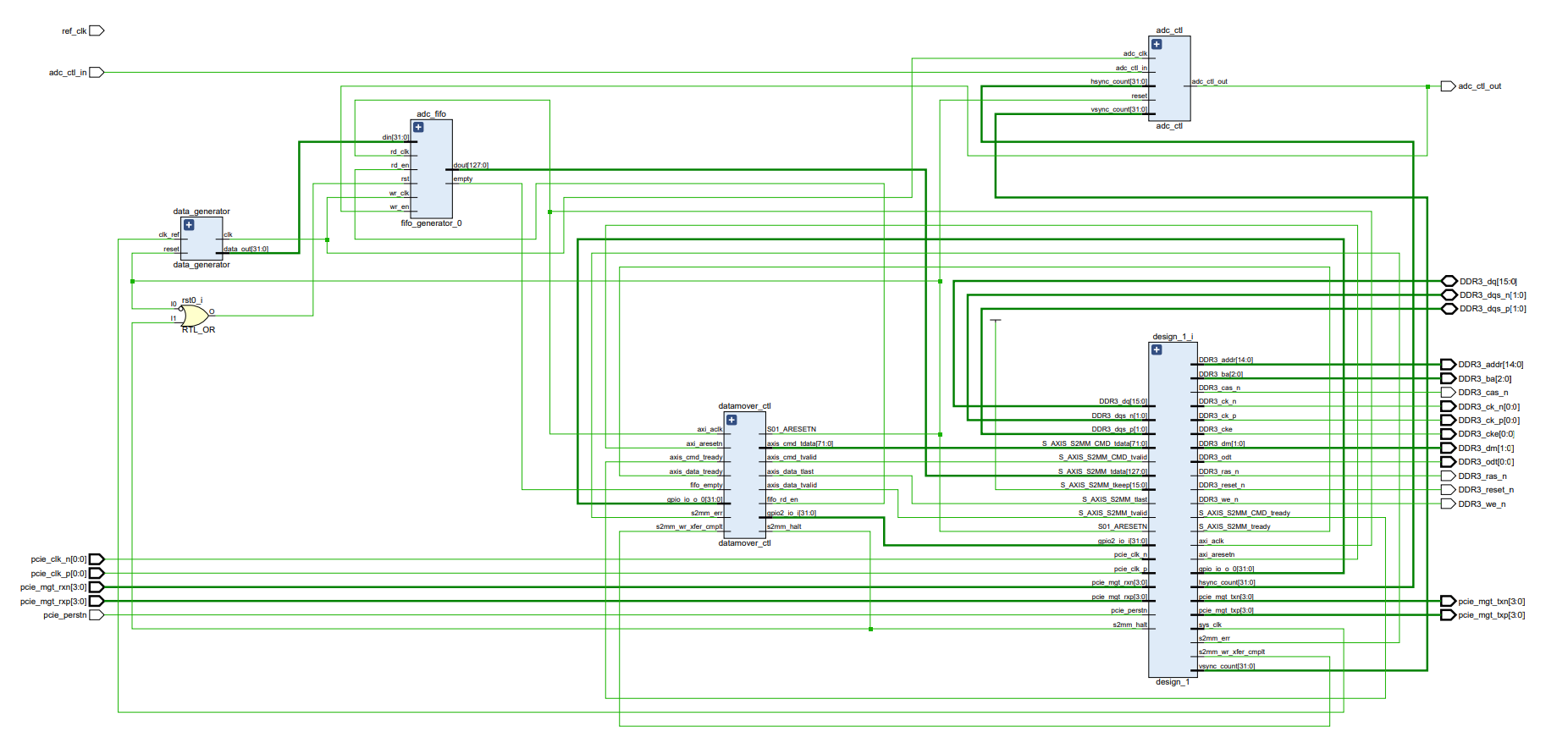 The pdf of the schematics is in the dso folder for those who hasn't mastered microscopic vision yet.
The data generator block is the temperary replacement for the actual adc channels. The input clk_ref is a 100MHz clock signal, the reset is active-low. The output clk is 80MHz.
The adc_ctl block implements the vsync and hsync controls. This is the problematic block we have. The block functions like a clock divider. The issue is with the initialization. I wanted it to initalize through the AXI_Lite port, but it's not behaving as expected.
The adc_fifo block buffers the incoming data and feeds the output into the datamover block in design_1. rd_clk is 125MHz, rd_en is high whenever data is available. rst is active-high. wr_en is from adc_ctl.
The datamover_ctl block ouputs the control signals used in datamover. I wanted to seperate the data path and the control components for a cleaner structure. Hence the adc_ctl and this module.
The design_1 block is largely from Alex's design. The design looks like this: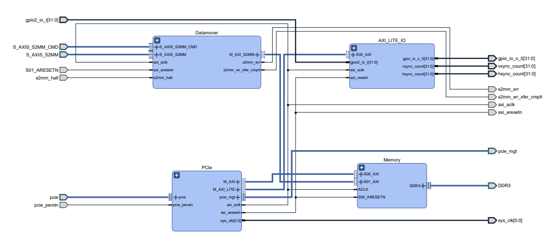 Again the pdf file is available.
The datamover is an interface for AXI stream to AXI data transfer.
The control interface provided by the AXI protocol. Alex's design had one AXI GPIO block inside the module (double click to open it). I added the second GPIO module to implement the sync controls. This should be a good starting point to debug the design.
An interface for both datamover and PCIe to communicate with the DRAM. Nothing to be modified for now. If a new DRAM layout is used in the future, the mapping needs to be changed in Memory/MIG 7/Property/Pin Selection
The module interfaces with the PCIe lane hardware.
Contrary to common beliefs, I did try to debug the program.
I striped away everything except the sync control components, did not work.
I hardcoded the vsync and hsync counts, and the design works.
The issue should be with the initialization step. The next thing I would do is tie the AXI GPIO output to the IO pins and see if the values are actually set properly. The more important thing is checking if the values are persistent. Since my design for the sync functionality relies upon the assumption that the GPIO outputs are.
My current suspision is that the device can't access AXI GPIO 1 (sync control parameters) while accessing AXI GPIO 0 (start, end, counter), since the two are connected to the same crossbar. If that is the case, maybe buffering AXI GPIO 1 as soon as the value is changed would help?
SelectIO Interface Wizard provides a really simple way to interface LVDS signals. The testing program should offer more insight to how to use it. The IOSTANDARD needs to be set accordingly in the constraint file. The reference I linked goes over the operations for reading the signals.
The software for communicating with the FPGA board.
- The CreateFile() syscall is used to create the device handle.
- The SetFilePointerEx() syscall moves the pointer to desired location.
- The base address of memory mapped components are set here.
 (No pdf for you this time) The two PCIe/xdma_0 mapped commponents are accessible from the PC side. After the device handle is created, the address is set to the base address. The M_AXI is called c2h0 and M_AXI_LITE is called user in the software. To access axi_gpio_1 the address needs to be incremented accordingly. Although like I mentioned before, the functionality needs to be tested still.
In memory mapped AXI (AXI3, AXI4 and AXI4-Lite), all transactions involve the concept of a target address within a system memory space and data to be transferred.
Memeory mapped systems often provide a more homogeneous way to view the system, because the IPs operate around a defined memory map.
The AXI4-Stream protocol is used for applications that typically focus on a data-centric and data-flow paradigm where the concept of an address is not present or not required. Each AXI4-stream acts as a single unidirectional channel for a handshake data flow.
At this lower level of operation (compared to the memory mapped AXI protocol types), the mechanism to move data between IP is defined and efficient, but there is no unifying address contet between IP. The AXI4-Stream IP can be better optimized for performance in data flow applications, but also tends to be more specialized around a given application space.
- DMA/Bridge Subsystem for PCI Express v4.1 Product Guide https://docs.xilinx.com/r/en-US/pg195-pcie-dma/IP-Facts
- AXI Reference Guide https://docs.xilinx.com/v/u/en-US/ug1037-vivado-axi-reference-guide
- AXI Tutorial https://github.com/absolutezero2730/AXI_DMA_FIFO
- AXI DataMover LogiCORE IP Product Guide https://docs.xilinx.com/r/en-US/pg022_axi_datamover
- AMBA AXI and ACE Protocol Specification https://developer.arm.com/documentation/ihi0022/e/AMBA-AXI3-and-AXI4-Protocol-Specification
- Serial LVDS High-Speed ADC Interface https://docs.xilinx.com/v/u/en-US/xapp524-serial-lvds-adc-interface
- SelectIO Interface Wizard Product Guide https://docs.xilinx.com/v/u/en-US/pg070-selectio-wiz