Hardware Design for LaunchXL-F28379D Control Interface Board for Power Electronics Application
(Voltage/Current Sensing, Precision References, and Hardware OCP)
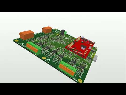
Open-source hardware companion board for TI’s LAUNCHXL-F28379D LaunchPad. Provides 6 isolated voltage channels, 6 current channels (3× AC, 3× DC), precision 1.5 V/3.0 V reference rails, and hard-wired window-comparator over-current protection with a latched DIS_Gate_Driver output. Designed with Altium 25.8.1 Included all callibration data. All functionality tested and working.
Safety notice: This hardware interfaces with high-energy power converters. Only qualified users should assemble and operate the board. Follow local electrical safety standards and isolation practices.
- Features
- Hardware overview
- Electrical characteristics
- Over-current protection (OCP)
- MCU pinout and integration
- Bring-up and calibration
- Known limitations
- License
- How to cite / reference
-
Power architecture
- 10–30 V input → 6.5 V/1 A preregulator
- AZ1117-ADJ LDOs generate 5 V and 3.3 V rails
- Test points and status LEDs on each rail
-
Precision references
- AZ431 (TL431-class) shunt references form 1.5 V and 3.0 V low-noise rails for sensor offsets and comparator ladders
-
Voltage sensing (6× isolated)
- AMC3330 isolation amplifiers (differential)
- TLV9001 diff-to-single-ended post-amp into 0–3.0 V ADC domain
- Clamp protection with BAT54S and RC anti-aliasing
-
Current sensing (6× total)
- AC: 3 channels, ±20 A, CT426-HSN820MR, 50 mV/A
- DC: 3 channels, 0–20 A, CT426-HSN820DR, 100 mV/A
- OPA4340 conditioning, offsets from 1.5 V/3.0 V refs, clamp/RC filters
-
Hardware protection
- Dual LMV393 window-comparators per AC current channel
- Latched fault via MC14044BDG; LED indication
- Discrete MOSFET drives DIS_Gate_Driver; Reset_OverCurrent_n clears latch
-
F28379D integration
- Fits LaunchPad BoosterPack headers (J1–J8)
- Dedicated PWM header (PWM1A/B … PWM6A/B)
- Lines for OverCurrent_Det, MCU_DIS_Gate_Driver, Reset_OverCurrent_n
- “Fault” and “Heartbeat/Run” LEDs
     16–30 V IN
         │
   R-78B6.5-1.0 ──► 6.5 V ──► AZ1117-ADJ ─► 5 V
                              AZ1117-ADJ ─► 3.3 V
               │
               ├─► AZ431 3.0 V REF ──┐
               └─► AZ431 1.5 V REF ─┴─► Offsets & comparator ladders
                                        (RC filtered, local decoupling)

HVx ──► AMC3330 (iso diff) ─► TLV9001 (SE) ─► ADCx (0–3.3 V, clamped)   ×6

AC Ix (±20 A, 50 mV/A) ─► OPA4340 chain ─► ADCx  ─► LMV393 window → MC14044 latch
DC Ix (0–20 A, 100 mV/A) ─► OPA4340 chain ─► ADCx            │
                                                           LED + DIS_Gate_Driver (MOSFET)
                                                           Reset_OverCurrent_n (MCU)
- Rails: 6.5 V (primary), 5 V, 3.3 V, 3.0 V-REF, 1.5 V-REF
- Test points: TP* per rail and key analog nodes
- LEDs: Power-good, Fault (latch), Heartbeat/Run (MCU)
| Item | Value / Range | Notes |
|---|---|---|
| Input supply | 10–30 V | |
| 6.5 V prereg | 1 A max | R-78B6.5-1.0 module |
| 5 V, 3.3 V rails | up to ~1 A ea | AZ1117-ADJ, local bulk + 0.1 µF decoupling |
| Reference rails | 1.5 V, 3.0 V (≈10 mA ea) | AZ431 shunts, RC filtered |
| Voltage sense | 6 channels, isolated | AMC3330 + TLV9001 |
| Current sense | 3× AC (±20 A, 50 mV/A), 3× DC (0–20 A, 100 mV/A) | CT426-HSN820MR/DR + OPA4340 |
| ADC domain | 0–3.3 V | Clamp: BAT54S |
| OCP thresholds (AC) | ±19.5 A (typ) | Window comparator about 0-current offset |
| Latch & disable | Latched OverCurrent_Det; DIS_Gate_Driver asserted | Reset via Reset_OverCurrent_n |
See the schematic PDF for final values.
Each AC channel feeds a dual LMV393 as a window comparator around the nominal zero-current offset. The resistor ladder derives upper/lower thresholds from V_{\text{REF_3V}} such that:
Use the provided resistor values in the schematic to reproduce the exact thresholds.
- Comparator asserts Low on MC14044BDG → OverCurrent_Det LED turns on → Can be read on MCU
- Latch drives MOSFET stage → DIS_Gate_Driver asserted (active high)
- MCU pulls Reset_OverCurrent_n low to clear latch and re-enable gates
- Reset_OverCurrent_n must be kept high by MCU to arm protection
Propagation from threshold crossing to DIS_Gate_Driver is purely hardware-bounded (no firmware in the loop).
LaunchPad headers J1–J8 carry ADC inputs, comparator/latch signals, and GPIOs. A separate PWM header carries PWM1A/B … PWM6A/B.
Pin maps: the exact ADC SOC channel to header pin mapping is provided in callibration folder. Import into your C2000 project to generate
#definemacros.
Firmware integration notes (C2000 / F28379D)
- Trigger ADC SOCs from ePWM at a fixed sampling phase; ensure sampling windows respect the RC time constant at each ADC input.
- Configure PPB (post-processing block) for offset subtraction if desired; otherwise subtract calibrated
$V_{\text{OFF}}$ in software. - Use a GPIO interrupt or polling on OverCurrent_Det for status logging; DIS_Gate_Driver is hardware-driven and should be honored by gate-driver logic.
- Visual inspection (polarity of electrolytics, diodes, orientation of AMC3330/OPAs/comparators, TL431 pins).
- Continuity on power rails; check for shorts to GND.
- No MCU installed; power with lab supply current-limited to ~500 mA.
- Apply 10–24 V at J-power.
- Verify 6.5 V, 5 V, 3.3 V, 3.0 V-REF, 1.5 V-REF at test points (±2%).
- Confirm LEDs illuminate as expected.
-
With inputs shorted or connected to known fixtures, measure each ADC node’s offset:
- AC current channels should sit near 1.56 V (design target).
- DC current channels near their configured 0 V.
-
Sweep the inputs (precision source or fixture) and record
$V_{\text{ADC}}$ vs.$V_{\text{IN}}$ or current; fit a line to obtain gain and offset.
Calibration model (per channel)
Callibration excel file is added with the project. Refer it for more information.
- With controlled current source, increase magnitude until OverCurrent_Det asserts.
- Confirm DIS_Gate_Driver goes active and latch holds after the stimulus is removed.
- Toggle Reset_OverCurrent_n to clear; confirm normal operation resumes.
- Record the measured trip points and compare with ±19.5 A targets.
- Small Offset (~0.08V) on DC Current null input. Fix: Compensate for the offset in the firmware. Callibration data provided.
- To arm the Over current protection the Reset_OverCurrent_n pin has to be pulled high by MCU.
- All RES and CAP package are 1206. 0.1uF are mistakenly described as 0805 package
This design is licensed under the Creative Commons Attribution 4.0 International License.

If this board contributes to your research or product:
@misc{ControlInterfaceBoardF28379D,
  title  = {Control-Interface Board for LAUNCHXL-F28379D: Voltage/Current Sensing, Precision References, and Hardware OCP},
  author = {Patel, Parth},
  year   = {2025},
  howpublished = {\url{https://github.com/parth-iitmandi/PowerRapidControlInterfaceHW}}
}